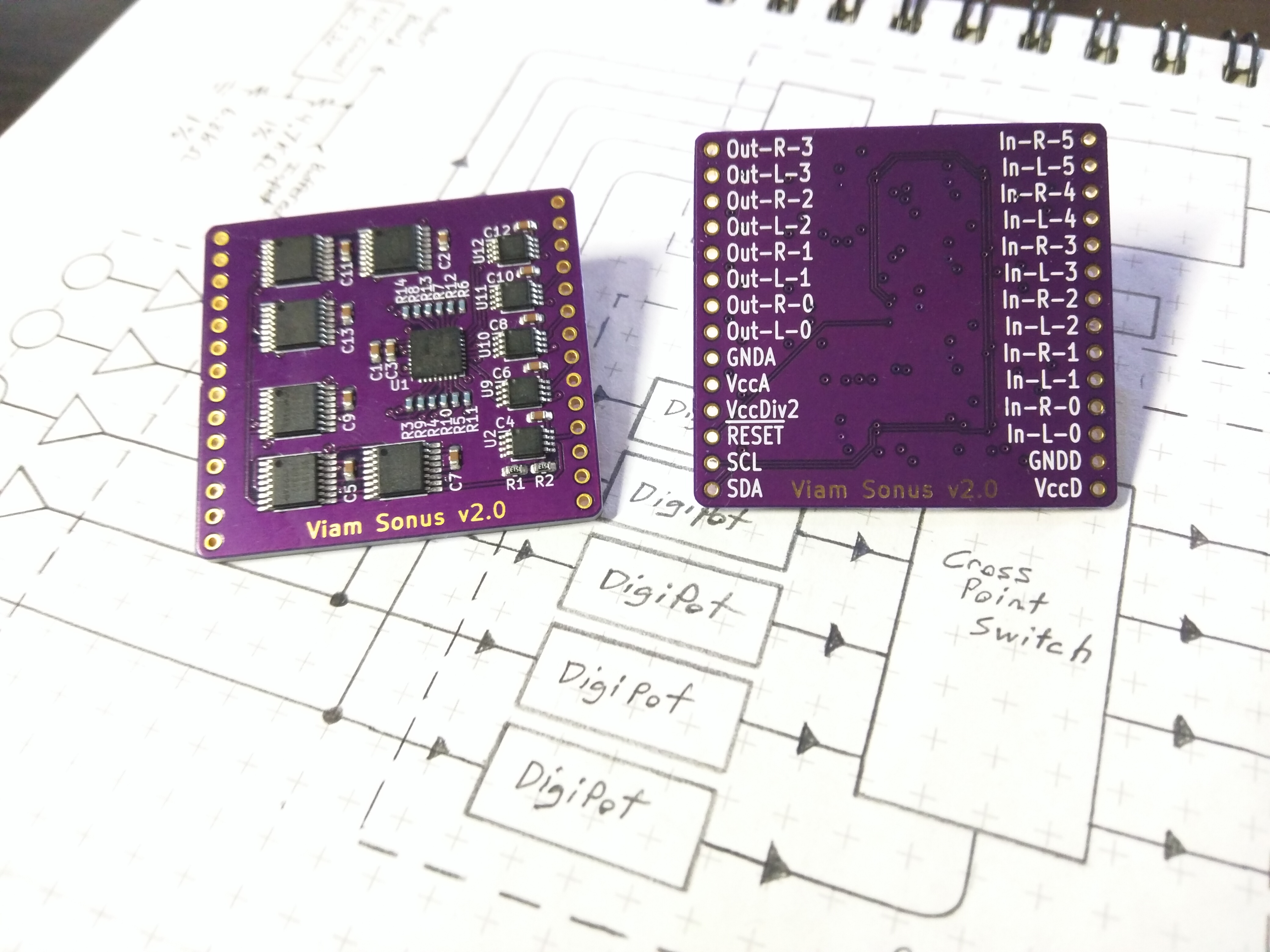
Viam Sonus 2.0
2019-11-16 14:45 by Ian
This is an improved version of my audio router board.
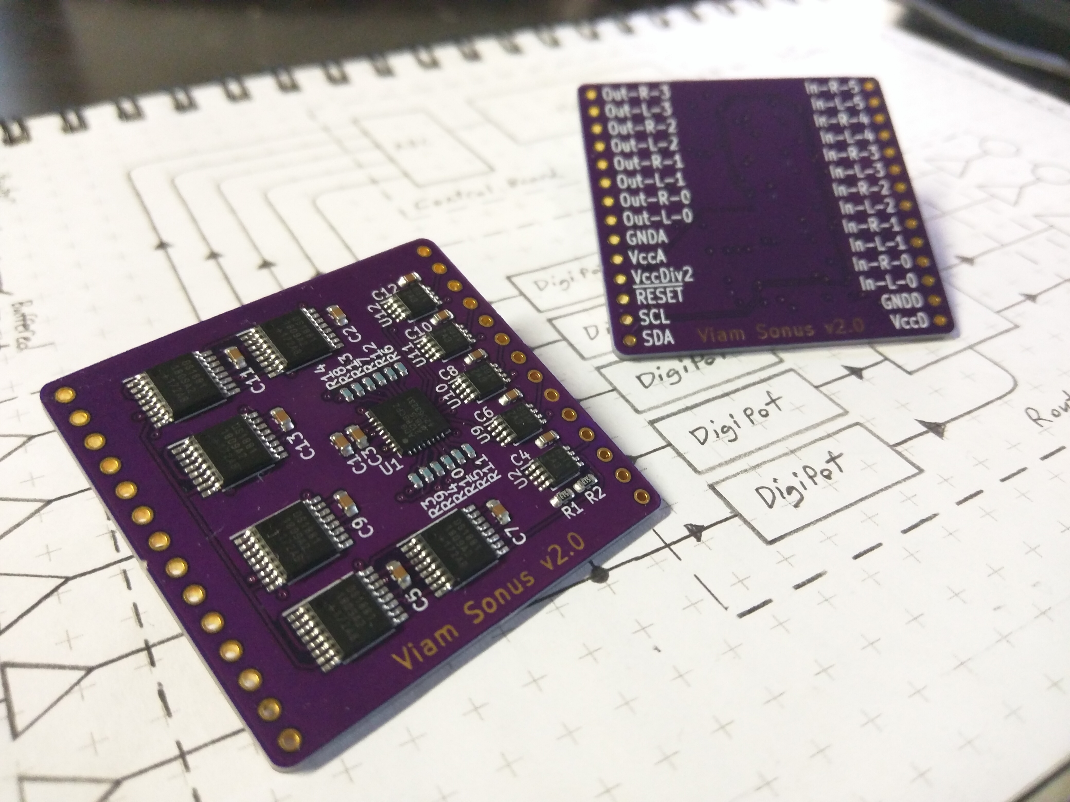
Features:
- 12 input channels that are arbitrarily routable to any of 8 output channels.
- Onboard digital potentiometers on the input side with non-volatile storage. Pots are logarithmic with zero-cross detection, and are paired in order with their input numbers on the board's silkscreen.
- Onboard op-amps on the output side with 300mA drive capability to provide buffering for direct-drive of line-level signals.
- Onboard buffered voltage divider with exposed output and 300mA drive capability to aid design and implementation of input buffers.
- Resistors added to the input-side of the switch, but after the potentiometers to allow for simple resistance mixing of signals simply by routing two inputs to a given output without risking damage. Some caveats apply (discussed below).
- Input-side is left free-form to allow use with single-ended (unbalanced) or differential (balanced) signals, and/or DC-biased sources.
- Safe for 5v audio signals.
- Isolated analog and digital power planes.
- Silkscreen reflects the envisioned usage (stereo signals), but the driver allows for easy grouping of any number of channels.
- Breadboard-friendly
| Repo | https://github.com/jspark311/ViamSonus-2.0 |
| Tindie | https://www.tindie.com/products/jspark311/viam-sonus-20/ |
| Hack-a-Day | https://hackaday.io/project/168501-viam-sonus-20 |
| Manuvr Driver | In progress (Elements stable) |
| Arduino Driver | Working, and gaining features |
Specs and requirements:
| Parameter | Minimum | Maximum | Recommended |
| Digital voltage range | 2.7v | 5.5v | 3v - 5v |
| Analog voltage range | 4.5v | 5.5v | 5v |
| Channel current | 1mA | ||
| Current requirements (Digital) | <5mA | ||
| Current requirement (Analog) Note 0 | 1mA | 2.7A |
Notes:
- 0: Analog current requirement depends strongly on draw from outputs and VccDiv/2 pin. Figures given are total board ranges.
Organization:
The router board has twelve inputs and eight buffered outputs.
The ADG2128 switch's analog performance is isotropic with respect to signal direction (row->column versus column->row). So I could have easily built the board to have eight inputs and twelve outputs. But there had to be a exclusive choice made due to the volume control orientation, even if not for the output buffers (which v1 didn't have).
The silkscreen reflects stereo usage, but neither the driver, nor the hardware are limited to this use. However, each stereo pair (as denoted by the silkscreen) corresponds to a single DS1881. Two independent mono channels can be independently attenuated by a single DS1881, but there is a means to adjust both halves of the DS1881 with a single i2c operation. So if a stereo channel is to be routed, the silk reflects the most efficient way of doing this.
The driver class (ViamSonus.h) ultimately manages channel bindings and co-routing. The API it presents works in terms of mono channels, with these relationships:
| Inputs | Outputs | ||||||||||||||||||||||||||||||||||||||||||||||||||||||||||||||||||||||||||||||||
|
|
Unlike v1 of this board, these relationships are continuous, orderly, and all ascending. During the driver porting effort, I was astounded at how much complexity fell away. Lookup tables and whole function chains were replaced with single line shifts and/or mask operations.
Interesting side-note: This simplification in software (and thus, the concomitant increase in reliability) costs about $5/board. Version 1.0 of this board was optimized for hardware routing in the PCB layout for the sake of being able to fit the circuit on 2-layers. This strategy functioned, but the patchwork in the driver class was so pervasive that it was difficult to understand, maintain, and carried runtime costs in the form of memory load for indirection tables and the CPU time to consult them.
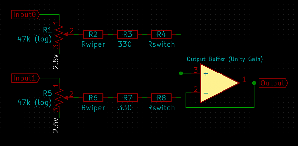
Mixing (applies also to ducking and crossfade):
The inputs are direct to the DS1881s with no biasing, current-limiting, or DC-blocking capacitors. This gives far more freedom to the end-user about the nature of the signals they can use the board with, but also means that it would be easy to burn out a channel. The default driver behavior is to disallow many-inputs-per-output. So if you are going to be using the board this way, please read this section carefully.
The ADG2128 driver will happily allow arbitrary connections between rows and columns. So the last version of this board didn't allow any form of mixing by software fiat. Since the volume control was on the output side, ratiometic mixing would have been impossible anyhow. The new design makes this possible because the volume control is on the input side, and the buffered outputs (alieviating any concerns over sink current) make it feasible to implement a summation mixer through the switch.
A practical consequence of this is that the volume can only be changed in one place (the input side). So mixing two input channels into a given output will mean potential volume changes on any other outputs to which the inputs are also connected.
The current through a given channel is the most important thing to consider when planning out your design and software. The potentiometer wipers are the weakest link, and under no circumstances should current through a wiper exceed 1mA in either direction. To that end, here are some facts about the hardware.
The version of the ADG2128 in this board is the "Y" version. Which has slightly slower switching times (about 15ns), and slightly higher switch resistances (a few ohms). But for this application, the more expensive "B" version wouldn't add any additional benefit.
Here is a model of the non-negligible resistances in the signal pathway through the router board. The first is a simple-case 1:1 connection. The second is 2:1 mix. It is assumed that VccA is the recommended value of 5v, and that input signals are biased about the midpoint of 2.5v.
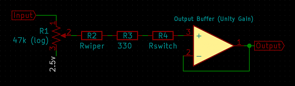
| Ref | Ω (min) | Ω (max) | Details |
| R1 | 0 | 45k | DS1881E fixed resistance, 20% tolerance. Note 1 |
| R2 | 160 | 250 | DS1881E wiper's intrinsic resistance at 5v. Note 2 |
| R3 | 327 | 333 | 1% tolerance 1/10w |
| R4 | 30 | 60 | Max current is ~20x higher than R2. Note 3 |
Notes:
- 1: This is the wiper's resistance range. Our model below will use an empirical table for the value of R11-2 and R12-3
- 2: The current through this resistor must never exceed 1mA.
- 3: ADG2128 datasheet value for minimum "on" resistance is not available for conditions of Vdd=+5v and Vss=0v. Additionally, the resistance of the switch is altered by how much current is moving through it, meaning this value changes with input signal. So the lowest non-differential value will be used for safety. In practice, this will be higher.
In the simple case (no mix), the resistance through a channel sums to no less than 517Ω. Under these conditions, there is no meaningful sink for the current, and negligible capacitance in the channel before the signal's arrival at the output buffer. Thus, no additional resistance is needed on the input side of the channel for signals at any voltage up to and including VccA.
Mixing operation is another matter because it allows current to flow via the first channel, and back into the source of the second channel. That is: there is a potential sink.
Even with biased and DC-blocked inputs, mixing could see a worst-case maximum (5v) differential across two input pins being joined at the far-side of the switch. Such would be the case for a full-volume mix of two inputs that are both at peak and are 180° out of phase.
With a 5v peak-to-peak signal, this gives a maximum voltage differential of 5v, and a total path resistance of 1044Ω. By Ohm's law, this gives a total channel current of 4.83mA, which would burn out the wiper. We need 5kΩ of total path resistance to be present as the signal peaks. We should divide this resistance evenly between the channels for 2.5kΩ of total resistance per-channel. With 517Ω already baked in at each channel, we should add a series resistance of at least 2kΩ to each channel that is to participate in mixing for no-fear operation. A 3.3v peak-to-peak signal would need to add about 1.1kΩ.
Example input/output circuit:
Here is the circuit I am using with this board. Further discussion of I/O circuits will have this in mind, unless stated otherwise.
Outputs:
The native arrangement of the outputs is for single-ended drive (IE, RCA and/or TRS jacks). A differential application output stage is presently beyond the scope of this post.
If you anticipate wanting to drive small speakers directly, you should use larger capacitor values on the output side. In my example circuit, I use 100uF electrolytics, and this is sufficient to drive my 26Ω headphones down to 50Hz with good results without sacrificing high-end. The capacitors will block DC flows, and thus prevent damage to the output buffers in the event of short-circuit. All that will happen is low drive volumes if your driven impedance falls too low. Each channel is good for 300mA at rail-to-rail voltage. So you'll have ample headroom.
Line level drive should also be DC blocked with a capacitor, but if you only expect to drive high-impedance inputs, you can get away with something smaller and cheaper without giving up low-end response.
Inputs:
The inputs will largely depend on what types of signal you want to accept. Ultimately, it would need to be converted into a single-ended signal centered about 2.5v (available on the VccA/2 pin). The easiest way to do this is by biasing and DC-blocking as shown in the example schematic.
Previous: The Woose Tracker
Next: Home VoIP System Part 0: Introduction and materials