2022.02.22: H-bridge deadband sequencer
2022-02-22 21:35 by Ian
One of the basic problems of H-bridge design is making sure that each MOSFET on a given leg of the bridge is only on while the other is off. If this gap (or "deadband") is not enforced by hardware, it must be done in firmware (if you have firmware).
Why does the H-bridge need a deadband?
YouTube user Josh Sideris has posted some excellent discourse on this topic, and H-bridges in general. So I will refer to these videos.
So I did this
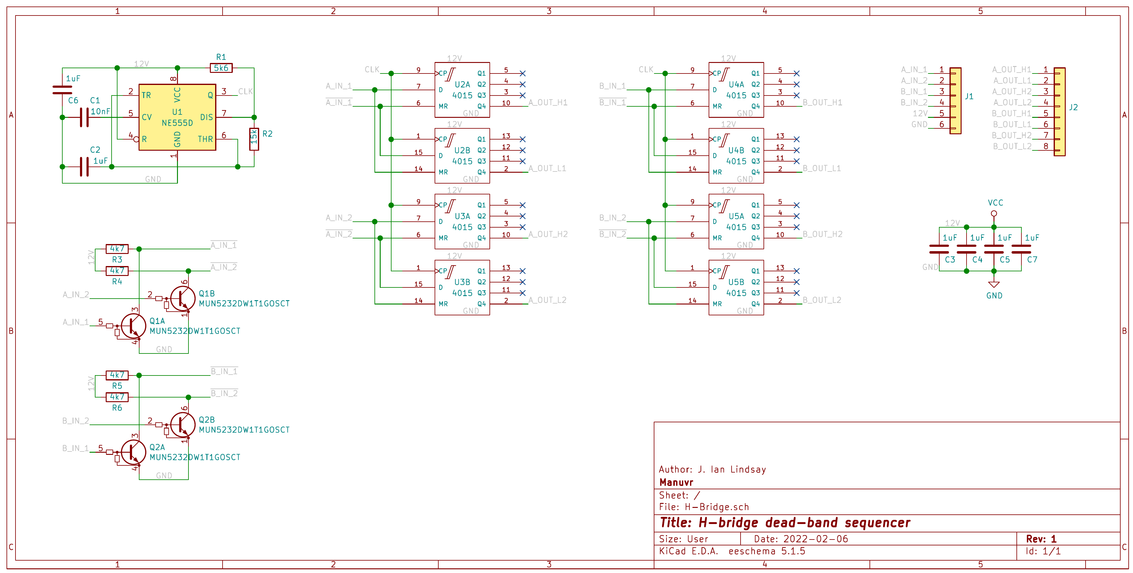
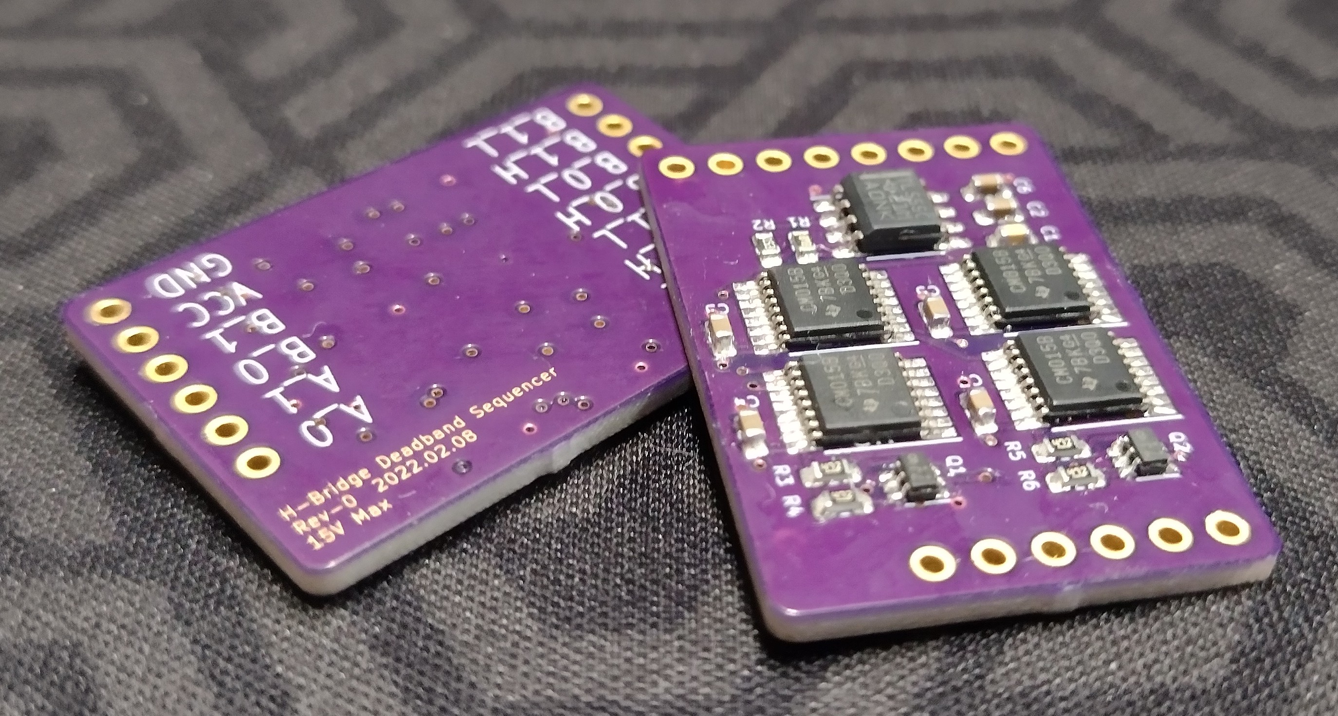
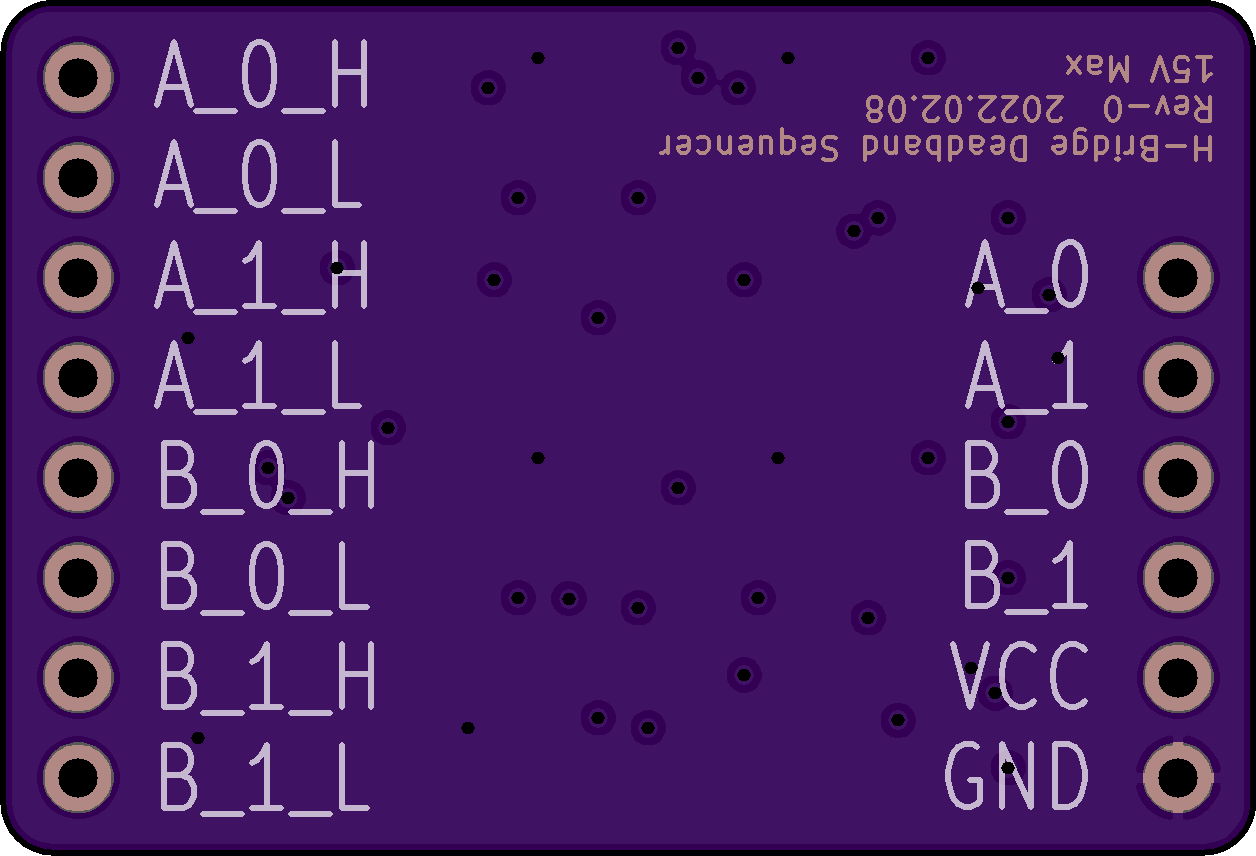
Trying to do this in firmware (while possible) feels like inviting a fire. Especially because doing it in hardware is so cheap. To that end, this is a logic-level front-end to an H-bridge that provides deadband enforcement. This particular circuit supports 4-channels; sufficient for two H-bridges.
Overview
- Supply range of 5-15V.
- Load capacity of output pins: 15mA
- The logic inputs are internally pulled low, thus assuring that the H-bridge initializes into a safe state (both load poles grounded).
Most H-bridge applications don't need the ability to set the load poles to a high-Z (undriven) state, so we accept that we can't do that, and thus reduce the input pin count to a single digital input per-leg. This allows the H-bridge to assume four stable states, which are selected by two input pins; each leg of the bridge being controlled by a single pin.
The voltage at each leg of a connected H-bridge mirrors the state of the respective logic input with differential delay (enforced by a shift register). Changing the state of the input will immediately inactivate the currently active half of the leg, and will only enable the opposing half after a delay of 3-4 clock cycles.
All outputs from this module are active-high, and are thus not suitable for direct-drive of the P-channel of a given leg. Intermediary transistors are required, as appropriate to the application.
Theory of operation
Each MOSFET is driven by a dedicated 4-bit shift register to implement a high-going delay. All shift registers are fed from the same clock, which is generated by a 555 timer in astable mode. The input condition that results in an undriven MOSFET will drive that shift register's RESET pin active, thus driving the output signal LOW asynchronously (immediately).
At the same time, the inverted version of the input signal is releasing the RESET line of the shift register that drives the complementary MOSFET; which will be enabled on the fourth clock pulse since RESET became dis-asserted.
The shift registers are required to ensure that a state change at an input that happens to coincide with a clock edge will not immediately propagate to the MOSFET to be driven active. A counter or sequence of 555 timers could also have served this role, but some measure needs to be taken to provide the assurance that the MOSFETs are not both active at the same time.
The length of the guaranteed deadband can thus be adjusted by choosing the RC values surrounding the timer. Default values were chosen that result in a minimum deadband width of 12ms. This is usually more than enough time for the VGS thresholds of the MOSFETs to not overlap, but some designs will want to specify a tighter or looser deadband.
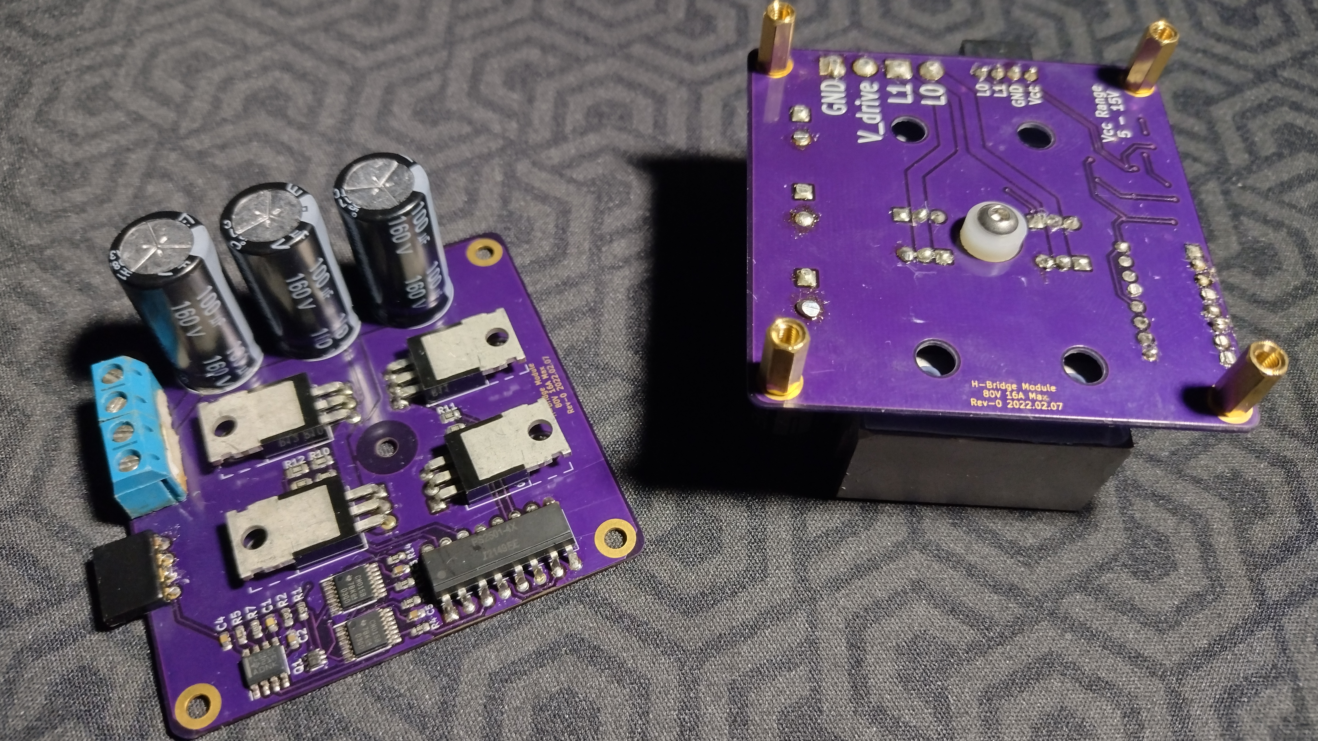
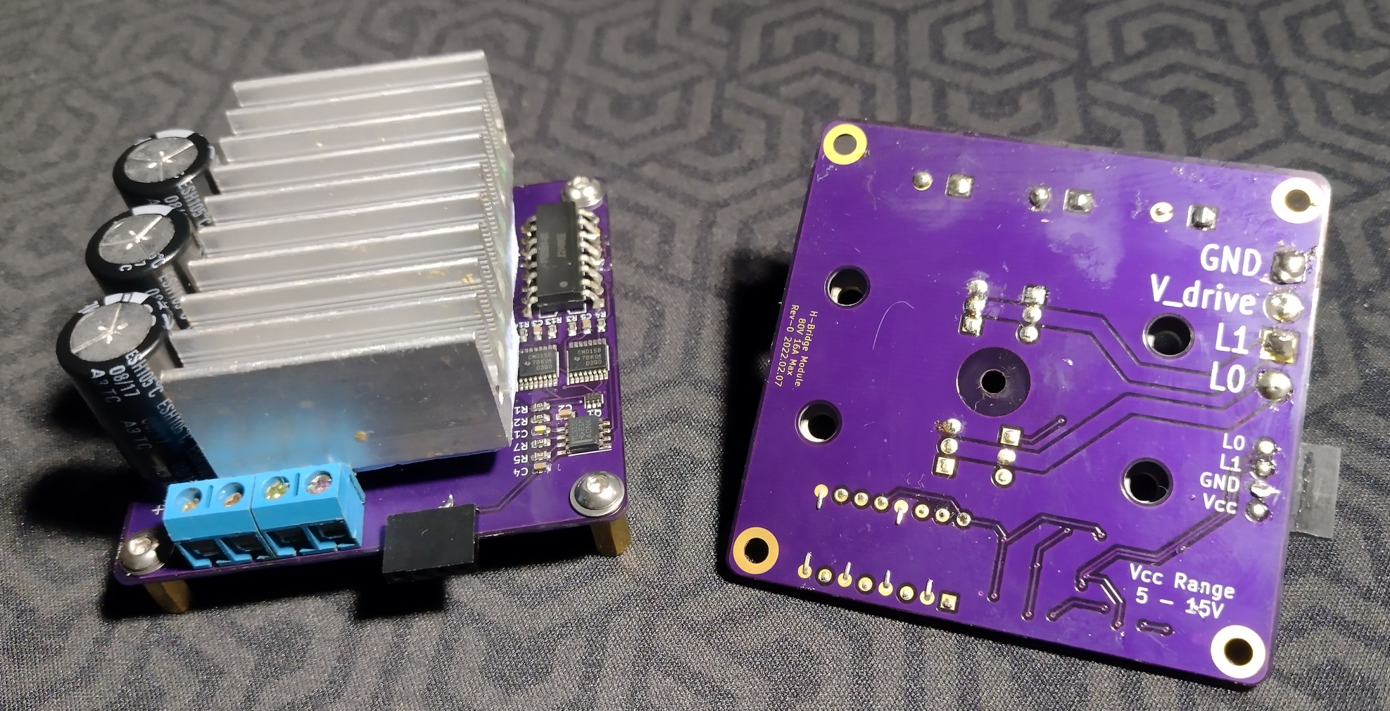
Pairing with driver circuitry
The board and schematic above is intended to sequence two H-bridges (A and B), but has no driver. The schematic below uses the same sequencer design, and pairs it with an optocoupler and four MOSFETs to form a complete H-bridge with built-in deadband enforcement.

 2021.09.05: LiPo reverse engineering